Diffractive optical waveguides are the key technology for Augmented and Virtual Reality (AR & VR) displays – they outperform competing solutions with their better field-of-view, smaller size and wider eye movement range. They are typically fabricated using nanoimprint lithography and reactive ion etching. This is a costly, time-
consuming and difficult process, requiring fabrication and very precise alignment of three different diffractive layers, one for each RGB colour.
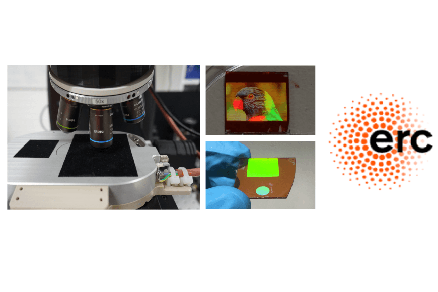
To tackle the problem we have developed a novel method for fabricating diffractive optical elements using light-induced sub-micrometre scale surface structuring of azobenzene-containing films. The method allows for creation of surface relief structures with varying heights and complex patterns, which are difficult to create using conventional lithography tools.
This is enabled by a novel a digital holographic microscope (DHM) tool that we developed for real-time, in-situ monitoring and feedback control of the surface-relief grating formation. The DHM instrument enables real-time observation of the surface relief grating formation with high spatial and temporal resolution, and the active feedback for an interference lithography addition we have devised enables control over the phase difference between the two interfering beams. Our approach - with precise control of pitch, direction and position (phase) of the sinusoidal pattern - allows an arbitrary one- or two-dimensional pattern to be created with multiple exposures by taking advantage of Fourier decomposition.
WE need to translate this or find a text
Impact
With our technology, we can reduce the manufacturing costs by eliminating the need of using e-beam
lithography for nanoimprint masters, as simple patterns can be overlaid to create complex surface textures.
The Holoshape method allows for faster prototyping of new topographies by replacing time-consuming cycle of pattern writing and transfer with one-step lithography on active materials. With the real-time feedback system it is possible to quickly identify faulty processes with precise monitoring of the surface topography. Typically for diffractive optical element (DOE) AR displays, the whole development period takes six months, whereas we believe with this method we can reduce the time needed to a few days, similar as with Holographic Optical Elements development process. Also, less materials are needed for prototyping because the surface topography can be erased and reconfigured as required. The materials used here have been studied over two decades and are widely commercially available.
Funding
Funding source
ERC Proof of Concept